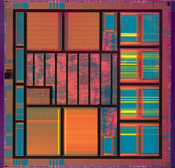


- Less than Half the Silicon Area of Other Designs
- Burst Memory Architecture Minimizes Cost
The J1 is a core cell design for an application specific signal processor which performs both Dolby AC-3 and MPEG audio decompression in a single design. The J1 is capable of decoding all AC-3 bitstreams with full support for bitstreams encoded with 5.1 channels and data rates of up to 640kb/s. The J1 downmixing capability produces stereo output in either normal or Pro-Logic compatible modes, making it ideal for DVD and set-top applications. For MPEG operation, J1 produces stereo output from either MPEG-1 or MPEG-2 audio bitstreams. The J1 audio quality meets the highest standards, allowing it to be used for the most demanding audio applications. The 20-bit PCM output yields Dolby ?Group A? performance for AC-3, and conforms to the highest audio quality level specified by ISO11172-4 for MPEG bitstreams. The J1 AC-3 decoding algorithm has undergone testing at Dolby Laboratories and has been qualified for Group A applications.
The J1 design is the world?s smallest, most cost effective design for AC-3 and MPEG audio decoding, and is less than half the size of designs employed by other vendors, such as ZORAN. The complete dual-standard J1 core is only 16-20K gates in size, and including ROM and RAM, requires a silicon area of less than 3mm2 in a 0.35u CMOS processes. While other designs incorporate multiple logic, RAM, and ROM blocks for various functions, the J1 uses only three blocks, one logic, one RAM, and one ROM, thereby minimizing inter-block routing overhead and silicon area. Because RAM is unified into a single block, the J1 is able to employ overlay techniques to reuse the RAM for multiple purposes, thus minimizing the number of bytes needed, and further reducing the silicon area. The J1 design incorporates all buffering and interface logic, so that it may be used in a wide variety of applications with no additional logic or buffering.
In order to achive the lowest incremental cost for audio decoding, J1 has been designed for efficient integration with other functions, like MPEG video decoding or PC graphics controller functions. This level of integration is enabled by J1?s glueless burst memory interface which allows the J1 to piggy back onto an internal memory bus and efficiently share DRAM memory with other functions. DRAM sharing allows on-chip RAM to be reduced by a factor of ten from what would otherwise be requried for the AC-3 and MPEG algorithms, thus minimizing cost. The burst memory interface is glueless, providing all memory addresses, and can be connected directly to a high speed memory bus without additional buffering. For efficient operation, all memory accesses are in blocks of 32 bytes, and J1 can tolerate latency inherent in shared memory systems. For non-integrated applications, the burst memory interface can be configured to directly address an on-chip SRAM.
Additional features are provided to support a wide variety of applications. For applications incorporating video, the J1 synchronization interface performs functions necessary for A/V synchronization with MPEG time stamps. For applications in automobiles or other noisy environments, the J1 core implements a dynamic range compression function which is compatible with Dolby Laboratories specifications. The J1 also provides stereo outputs which are ProLogic compatible. For DVD applications, the J1 provides PCM mode processing; with left, right, left+right (mono), volume control, and pass through modes. The J1 core also performs AC-3/MPEG framing necessary for interfacing to S/PDIF equipped external decoding devices. An optional output module provides the single wire S/PDIF serial output.
The J1 design kit is compatible with Synopsys and Verilog design methodology. J1 requires 0.5 micron or better technology, and is designed for synthesis with off-the-shelf gate array or standard cell ASIC libraries.
Combining the J1 with the Jacobs Pineda, Inc. JDA1 DAC/PLL core, a complete audio decoding subsystem can be built for DVD applications, accepting AC-3/MPEG digital audio in, and producing analog and SPDIF outputs with a single clock source.
About Jacobs Pineda, Inc.: JPI is a VLSI design firm specializing in high volume, cost sensitive, consumer audio IC designs. Its designs for DAC, PLL, AC-3, and MPEG applications have been licensed and employed by semiconductor and system manufacturers of audio solutions for the consumer and computing markets. Founded in 1995, JPI is a California Corporation with operating facilities in Oakland and San Francisco. More information can be obtained on their web site at http://www.jacobspineda.com.
For Information Contact: Steven A. Brightfield Centamicron, Inc. (415) 948-9293 brighty@jacobspineda.com
(c) 1997 Jacobs Pineda, Inc. All rights reserved.